top of page


Functional Gate Insulator and Interface Engineering for High-Mobility TFTs

In recent years, oxide semiconductors have superior electrical properties, low thermal budgets, and uniformity across large areas render them essential for advanced electronic technologies. Nevertheless, attaining a mobility exceeding 100 cm2/Vs remains challenging, which positions In2O3 with its large 5s orbital as a promising candidate to overcome this limitation.
In this study, the device exhibited the best performance, with effective defect passivation and an optimal carrier concentration, resulting in a high mobility of 148.12 cm2/Vs, moderate Von of −0.85 V, and Von shift of 0.44 V under PBTS condition
[1] Kim, H. Y. et al (2025). Optimized hydrogen-supplying gate insulator for high-mobility indium oxide TFTs via atomic-level oxygen reactant engineering. Journal of Alloys and Compounds, 1020, 179353.
Next generation device structure : Trench TFT


Oxide thin-film transistors (TFTs) with high mobility that exceed 100 cm2/V·s and appropriate turn-on voltage (Von) are necessary to drive next-generation displays and memory devices. However, a trade-off relationship exists between mobility and Von, making it difficult to achieve both in the same oxide TFT. In this letter, we propose a buffer layer engineered trench-TFT (T-TFT) as a solution to this trade-off problem. Trench TFT shows a high mobility of 129 cm2/V·s and a suitable Von of −0.4 V.
Trench-structured thin-film transistors (TFTs) based on oxide semiconductors have attracted increasing attention for next-generation high-resolution displays, owing to their compact footprint and potential for high current driving capability in short-channel configurations. However, oxide TFTs often suffer from negative threshold voltage shifts, which pose further design challenges.
In this trench TFT, the horizontally thick regions of the active layer function as highly conductive current paths, whereas the vertically thin regions serve as effective channels, which result in an on-current boosting effect. The device exhibited a favorable SS of 0.108 V/dec and reasonable Von of −0.68 V.
[1] Y. Im et al. (2023). Buffer Layer Engineering of Indium Oxide Based Trench TFT for Ultra High Current Driving", IEEE Electron Device Letters.
[2] Kim, D. H.et al (2025). Atomic layer deposition-enabled trench oxide thin-film transistors with selective dry etching for high-current driving applications. Journal of Alloys and Compounds, 184565.
Oxide semiconductor cation compostion control via PEALD
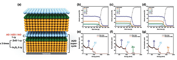
Ga has been widely used as a carrier suppressor in oxide semiconductors; however, research has recently been conducted to replace it with Al, which is cheaper and forms a stronger bond with O. In this study, an InAlZnO (IAZO) semiconductor was deposited using super-cycle PEALD for the first time. AlO (AO), AlZnO (AZO), and InAlO (IAO) as Al doping layers in IAZO are evaluated. Finally, the high-Al IAZO system using AZO successfully showed overall excellent properties including mobility over 10 cm2/Vs, and outstanding stability under 0.1 V, which are greatly improved compared to previously reported IAZO TFTs.
[1] Woo, N. et al (2023). Optimal aluminum doping method in PEALD for designing outstandingly stable InAlZnO TFT. Advanced Materials Interfaces, 10(12), 2300128


Self-Aligned TFT
Top-gate self-aligned structured oxide thin-film transistors (TFTs) are suitable for the backplanes of high-end displays because of their low parasitic capacitances. The gate insulator (GI) deposition process should be carefully designed to manufacture a highly stable, high-mobility oxide TFT, particularly for a top-gate structure. In this study, a nanometer-thick Al2O3 layer via plasma-enhanced atomic layer deposition (PE-ALD) is deposited on the top-gate bottom-contact structured oxide TFT as the interface tailoring layer, which can also act as the hydrogen barrier to modulate carrier generation from hydrogen incorporation into the active layer of the TFT during the following process such as post-annealing.
[1] J. B. Ko et al. "Engineering a sub-nanometer interface tailoring layer for precise hydrogen incorporation and defect passivation for high-end oxide thin-film transistors", ACS Applied Materials & Interfaces, 2023


Flexible and deformable Thin Film Transistor
Thin-film transistors (TFTs) are utilized as the backplane devices for active matrix (AM) liquid-crystal displays, AM organic light-emitting diode (AMOLED) displays, AM-LEDs, and quantum-dot LEDs. TFTs with amorphous oxide semiconductors are suitable candidates for such applications owing to their multiple advantages such as ease of fabrication, high electron mobility, high electrical stability, and uniformity over a large area. Therefore, it is necessary to develop flexible and transparent oxide TFTs that exhibit outstanding electrical performances. Furthermore, it is essential to design ultrathin display devices to ensure their complete coverage on and attachment to various objects including stretchable substrates.
[1] J. B. Ko et al. "Ultrathin, Flexible, and Transparent Oxide Thin-FIlm Transistors by Delamination and Transfer methods for Deformable DIsplays", Adv Mater Tech, 2021
bottom of page